- 您现在的位置:买卖IC网 > Sheet目录694 > MAX17009GTL+ (Maxim Integrated)IC CTLR VIDEO SERIAL DUAL 40TQFN
�� �
�
�AMD� Mobile� Serial� VID� Dual-Phase�
�Fixed-Frequency� Controller�
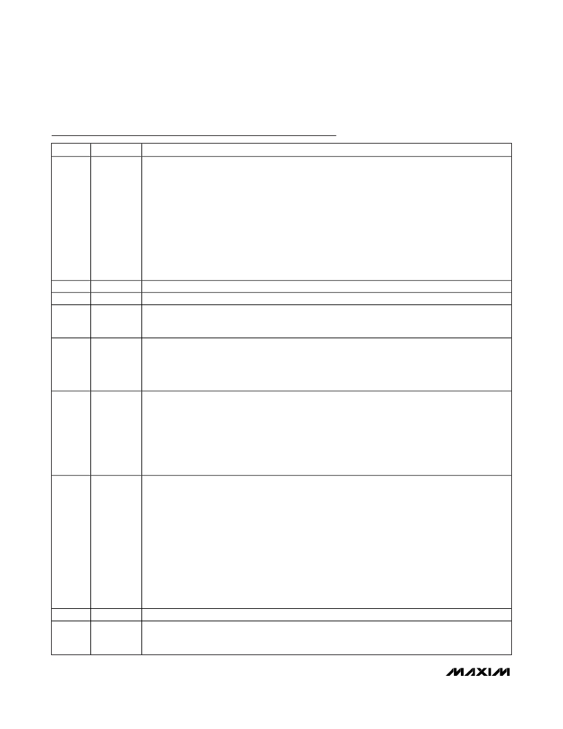
�Pin� Description� (continued)�
�PIN�
�7�
�8�
�9�
�10�
�11�
�12�
�13�
�14�
�15�
�NAME�
�TIME�
�SVC�
�SVD�
�THRM�
�GNDS2�
�FBDC2�
�FBAC2�
�V� DDIO�
�GNDS_NB�
�FUNCTION�
�Slew-Rate� Adjustment� Pin.� Connect� a� resistor� R� TIME� from� TIME� to� GND� to� set� the� internal� slew� rate:�
�PWM� Slew� rate� =� (6.25mV/μs)� x� (143k� Ω� /� R� TIME� )�
�NBV_BUF� Slew� rate� =� (7μA)� x� (143k� Ω� /� R� TIME� )� /� C� NBV_BUF�
�where R� TIME� is between 35.7k� Ω� and 357k� Ω� for corresponding slew rates between 25mV/μs to 2.5mV/μs,�
�respectively,� for� the� SMPSs,� and� NBV_BUF� currents� between� 28μA� and� 2.8μA,� respectively,� for� the�
�NBV_BUF.�
�This slew rate applies to both upward and downward VID transitions, and to the transition from boot mode�
�to� VID� mode.� Downward� VID� transition� slew� rate� can� appear� slower� because� the� output� transition� is� not�
�forced� by� the� SMPS.�
�The� SMPS� slew� rate� for� startup� and� shutdown� is� fixed� at� 1mV/μs.�
�The� NBV_BUF� slew� rate� is� the� same� during� startup,� shutdown,� and� normal� VID� transitions.�
�Serial VID Clock. During the power-up sequence and in debug mode, SVC is the MSB of the 2-bit VID DAC.�
�Serial� VID� Data.� During� the� power-up� sequence� and� in� debug� mode,� SVD� is� the� LSB� of� the� 2-bit� VID� DAC.�
�Input� of� Internal� Comparator.� Connect� the� output� of� a� resistor-� and� thermistor-divider� (between� V� CC� and�
�GND)� to� THRM.� Select� the� components� so� the� voltage� at� THRM� falls� below� 1.5V� (30%� of� V� CC� )� at� the�
�desired� high� temperature.�
�SMPS2� Remote� Ground-Sense� Input.� Normally� connected� to� GND� directly� at� the� load.� GNDS2� internally�
�connects� to� a� transconductance� amplifier� that� fine� tunes� the� output� voltage� compensating� for� voltage�
�drops� from� the� regulator� ground� to� the� load� ground.�
�Connect� GNDS2� above� 0.9V� combined-mode� operation� (unified� core).� When� operating� in� combined�
�mode,� GNDS1� is� used� as� the� remote� ground-sense� input.�
�Output� of� the� DC� Voltage-Positioning� Transconductance� Amplifier� for� SMPS2.� Connect� a� resistor� R� FBDC2�
�between� FBDC2� and� the� positive� side� of� the� feedback� remote� sense� to� set� the� DC� steady-state� droop�
�based� on� the� voltage-positioning� gain� requirement:�
�R� FBDC2� =� R� DROOPDC� /� (R� SENSE2� x� G� m(FBDC2)� )�
�where� R� DROOPDC� is� the� desired� voltage� positioning� slope� and� G� m(FBDC2)� =� 1mS� typ.� R� SENSE2� is� the�
�value� of� the� current-sense� resistor� that� is� used� to� provide� the� (CSP2,� CSN2)� current-sense� voltage.�
�To� disable� the� load-line,� short� FBDC2� to� the� positive� remote-sense� point.�
�FBDC2� is� high� impedance� in� shutdown.�
�Output� of� the� AC� Voltage-Positioning� Transconductance� Amplifier� for� SMPS2.� The� resistance� between�
�this� pin� and� the� positive� side� of� the� remote-sensed� output� voltage� sets� the� transient� AC� droop:�
�R� FBAC2� =� R� DROOPAC� /� (R� SENSE2� x� G� m(FBAC2)� )�
�where� R� DROOPAC� is� the� transient� (AC)� voltage-positioning� slope� that� provides� an� acceptable� tradeoff�
�between stability and load transient response, G� m(FBAC2)� and R� SENSE2� is the value of the current-sense�
�resistor� that� is� used� to� provide� the� (CSP2,� CSN2)� current-sense� voltage.�
�The� maximum� difference� between� transient� (AC)� droop� and� DC� droop� should� not� exceed� ±80mV� at� the�
�maximum� allowed� load� current� (DC� droop� is� set� at� the� FBDC2� pin).�
�Internally, V(FBDC2 - GNDS2) goes to the internal voltage integrator (slow DC loop), whereas V(FBAC2 -�
�GNDS2)� goes� to� the� error� comparator� (fast� transient� loop).�
�FBAC2� is� high� impedance� in� shutdown.�
�Note:� The� AC� and� DC� droop� cannot� be� different� by� more� than� ±3mV/A.�
�CPU� I/O� Voltage� (1.8V� or� 1.5V).� Logic� thresholds� for� SVD� and� SVC� are� relative� to� the� voltage� at� V� DDIO� .�
�North� Bridge� Feedback� Remote-Sense� Input,� Negative� Side.� Normally� connected� to� GND� directly� at� the�
�load. GNDS_NB internally connects to a transconductance amplifier that fine tunes the NBV_BUF output�
�voltage� compensating� for� voltage� drops� from� the� regulator� ground� to� the� load� ground.�
�16�
�______________________________________________________________________________________�
�发布紧急采购,3分钟左右您将得到回复。
相关PDF资料
MAX17410GTM+
IC CTLR QPWM 2PH FOR IMV 48TQFN
MC2711H
SWITCH BUSHING PLUNGER W/SEAL
MC2711
SWITCH BUSHING MOUNT PLUNGER
MC7711
SWITCH BUSHING MOUNT PLUNGER
MCA7711
SWITCH BUSHING MOUNT PLUNGER
MCD2711
SWITCH BUSHING MOUNT PLUNGER
MCD7711
SWITCH BUSHING MOUNT PLUNGER
MCZ2010AH900
CHOKE COMMON MODE 90 OHM SMD
相关代理商/技术参数
MAX17009GTL+T
功能描述:其他电源管理 AMD Dual-Phase CPU Controller RoHS:否 制造商:Texas Instruments 输出电压范围: 输出电流:4 mA 输入电压范围:3 V to 3.6 V 输入电流: 功率耗散: 工作温度范围:- 40 C to + 110 C 安装风格:SMD/SMT 封装 / 箱体:VQFN-48 封装:Reel
MAX1700EEE
功能描述:直流/直流开关转换器 1-3 Cell 1A Step-Up DC/DC Converters RoHS:否 制造商:STMicroelectronics 最大输入电压:4.5 V 开关频率:1.5 MHz 输出电压:4.6 V 输出电流:250 mA 输出端数量:2 最大工作温度:+ 85 C 安装风格:SMD/SMT
MAX1700EEE+
功能描述:直流/直流开关转换器 1-3 Cell 1A Step-Up DC/DC Converters
RoHS:否 制造商:STMicroelectronics 最大输入电压:4.5 V 开关频率:1.5 MHz 输出电压:4.6 V 输出电流:250 mA 输出端数量:2 最大工作温度:+ 85 C 安装风格:SMD/SMT
MAX1700EEE+T
功能描述:直流/直流开关转换器 1-3 Cell 1A Step-Up DC/DC Converters RoHS:否 制造商:STMicroelectronics 最大输入电压:4.5 V 开关频率:1.5 MHz 输出电压:4.6 V 输出电流:250 mA 输出端数量:2 最大工作温度:+ 85 C 安装风格:SMD/SMT
MAX1700EEE-T
功能描述:直流/直流开关转换器 1-3 Cell 1A Step-Up DC/DC Converters RoHS:否 制造商:STMicroelectronics 最大输入电压:4.5 V 开关频率:1.5 MHz 输出电压:4.6 V 输出电流:250 mA 输出端数量:2 最大工作温度:+ 85 C 安装风格:SMD/SMT
MAX17010AETL+
功能描述:LCD 驱动器 Internal-Switch Boost Regulator RoHS:否 制造商:Maxim Integrated 数位数量:4.5 片段数量:30 最大时钟频率:19 KHz 工作电源电压:3 V to 3.6 V 最大工作温度:+ 85 C 最小工作温度:- 20 C 封装 / 箱体:PDIP-40 封装:Tube
MAX17010AETL+T
功能描述:LCD 驱动器 Internal-Switch Boost Regulator RoHS:否 制造商:Maxim Integrated 数位数量:4.5 片段数量:30 最大时钟频率:19 KHz 工作电源电压:3 V to 3.6 V 最大工作温度:+ 85 C 最小工作温度:- 20 C 封装 / 箱体:PDIP-40 封装:Tube
MAX17010ETL+
功能描述:LCD 驱动器 Internal-Switch Boost Regulator RoHS:否 制造商:Maxim Integrated 数位数量:4.5 片段数量:30 最大时钟频率:19 KHz 工作电源电压:3 V to 3.6 V 最大工作温度:+ 85 C 最小工作温度:- 20 C 封装 / 箱体:PDIP-40 封装:Tube